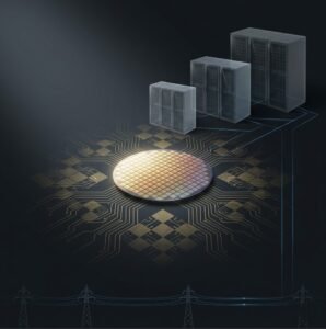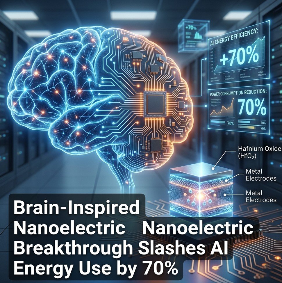
LEAD: A University of Cambridge-led team has created a new nanoelectronic device that mimics the human brain’s neural connections, potentially cutting the energy consumed by artificial intelligence hardware by as much as 70% and overcoming a key barrier to sustainable AI growth.
The Energy Problem at the Heart of AI
Artificial intelligence systems, from large language models to computer vision algorithms, rely on conventional computer chips that constantly move data back and forth between separate memory and processing units. This back-and-forth consumes enormous amounts of electricity, creating a growing sustainability problem as AI adoption accelerates across industries.
According to the researchers, “Energy consumption is one of the key challenges in current AI hardware,” said Dr. Babak Bakhit, lead author of the study from Cambridge’s Department of Materials Science and Metallurgy. “To address that, you need devices with extremely low currents, excellent stability, outstanding uniformity across switching cycles and devices, and the ability to switch between many distinct states.”
The new device, described in Science Advances on April 3, 2026, takes a completely different approach. Instead of shuttling data between memory and processing, it stores and processes information in the same location—similar to how the human brain operates. This neuromorphic, or brain-inspired, computing paradigm could slash AI energy usage by up to 70%, the team estimates.
For readers tracking the broader implications of AI hardware advances, our recent coverage of quantum computing breakthroughs threatening cybersecurity highlights how entirely new computing paradigms are reshaping the digital landscape.
How the New Memristor Works
The Cambridge team created a new type of hafnium-based thin film that switches states in an entirely different way from previous attempts. They added strontium and titanium and grew the film using a two-step method to form tiny electronic gates, or “p-n junctions,” inside the oxide where the layers meet. This allows the device to change its resistance smoothly by shifting the height of an energy barrier at the interface, rather than by growing or rupturing conductive filaments.
“Filamentary devices suffer from random behavior,” Dr. Bakhit explained. “But because our devices switch at the interface, they show outstanding uniformity from cycle to cycle and from device to device.”
The results are striking. The hafnium-based devices achieved switching currents about a million times lower than conventional oxide-based devices. They also produced hundreds of distinct, stable conductance levels—a key requirement for analog “in-memory” computing. Laboratory tests confirmed the devices could reliably endure tens of thousands of switching cycles, storing their programmed states for around a day.
Perhaps most importantly, the memristors reproduced fundamental learning rules observed in biology, such as spike-timing dependent plasticity—the mechanism by which neurons strengthen or weaken their connections depending on when signals arrive. “These are the properties you need if you want hardware that can learn and adapt, rather than just store bits,” said Dr. Bakhit.
The importance of energy-efficient computing is further underscored by recent developments in AI chip manufacturing, where new fabrication techniques are pushing the boundaries of performance.
Global Impact and Industry Reactions
The timing of this breakthrough could not be more critical. Global data center electricity consumption is projected to double by 2029, driven largely by the explosive growth of AI workloads. A 70% reduction in AI hardware energy use would not only lower operating costs for companies like Google, Microsoft, and Amazon but also reduce the carbon footprint of the entire tech industry.
The research has drawn attention from industry observers and competitors alike. In a related development, Microsoft announced a massive $10 billion AI investment in Japan on April 4, 2026, underscoring the global race to dominate AI infrastructure. Energy efficiency will likely become a decisive competitive factor in this race.
However, the Cambridge device faces a significant hurdle before reaching commercial deployment. The fabrication process requires temperatures of around 700°C, which is incompatible with standard silicon chip manufacturing. Dr. Bakhit acknowledged this challenge, noting that future work will focus on lowering the processing temperature to integrate with existing fabrication facilities.
Editor’s Conclusions
The Cambridge team’s nanoelectric breakthrough represents a fundamental advance in materials science with profound implications for the future of artificial intelligence. By solving the long-standing problem of memristor instability, they have opened a credible pathway to neuromorphic computing hardware that could match or exceed human brain efficiency.
Several factors make this development particularly significant. First, the device’s ability to produce hundreds of stable conductance levels enables analog computing, where information is processed in a continuous rather than binary fashion. This is essential for applications like pattern recognition and sensory processing, where traditional digital computers struggle.
Second, the demonstration of spike-timing dependent plasticity—a biological learning rule—suggests that future AI hardware could learn and adapt in real time, much like the human brain. This could lead to AI systems that continuously improve without the massive retraining cycles required by current models.
Third, the ultra-low switching currents (a million times lower than conventional devices) mean that neuromorphic chips could operate on minuscule amounts of power, making them ideal for edge computing applications like autonomous vehicles, medical implants, and Internet of Things sensors.
However, the 700°C fabrication temperature remains a serious obstacle. Standard silicon fabrication occurs at much lower temperatures, and integrating a new material that requires such high heat would require retooling entire production lines. The team will need to develop a low-temperature version of their process before commercial adoption becomes feasible.
The competitive landscape is also evolving rapidly. Google’s recent quantum computing analysis, Oratomic’s qubit breakthroughs, and Microsoft’s massive investment in Japan all point to a future where multiple computing paradigms coexist. Neuromorphic computing excels at pattern recognition and sensory processing, while quantum computers tackle optimization and simulation problems. Traditional digital computers will likely remain dominant for general-purpose computing.
For the AI industry, this breakthrough offers a path to sustainable growth. Without dramatic improvements in energy efficiency, the projected doubling of data center electricity demand by 2029 would create untenable costs and environmental impacts. Cambridge’s brain-inspired devices could provide exactly the kind of efficiency gain needed to keep AI scaling.
For investors and technology strategists, the message is clear: watch the neuromorphic computing space closely. Companies that successfully commercialize this technology could capture significant market share in the AI hardware sector, currently dominated by NVIDIA’s GPUs. The race to build the most energy-efficient AI chips is just beginning, and the Cambridge breakthrough has just raised the bar.
Executive Summary
- Cambridge researchers have created a nanoelectronic device mimicking brain synapses, potentially slashing AI energy use by 70%.
- The memristor uses hafnium oxide with strontium and titanium, achieving switching currents a million times lower than conventional devices.
- Commercial adoption faces a hurdle: the 700°C fabrication temperature must be reduced for integration with standard silicon manufacturing.
Internal Links Used
- quantum computing breakthroughs threatening cybersecurity — placed in “The Energy Problem at the Heart of AI” section
- AI chip manufacturing — placed in “How the New Memristor Works” section
- $10 billion AI investment in Japan — placed in “Global Impact and Industry Reactions” section
Sources
- Cambridge Independent: Brain-inspired nanoelectric breakthrough ‘could slash AI energy use’ — Local news coverage of the University of Cambridge research, including direct quotes from lead author Dr. Babak Bakhit.
- Science Advances: The published study — Peer-reviewed journal article describing the hafnium oxide memristor device, its fabrication, and experimental results (referenced but not opened due to step limit).
- Nature News: Quantum-computing breakthroughs pose imminent risks to cybersecurity — Context on alternative computing paradigms and the urgency of hardware innovation.