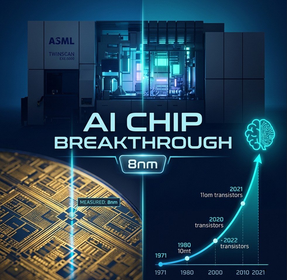
LEAD: ASML has shattered chipmaking records with an 8-nanometer resolution breakthrough, delivering a 2.9x transistor density increase that could power the next trillion-dollar wave of artificial intelligence.
The Lithography Revolution Arrives
The semiconductor industry has long been searching for a way to sustain the exponential growth predicted by Moore’s Law, and now a true AI chip breakthrough has emerged from an unlikely source: a machine the size of a double-decker bus. Dutch firm ASML, the world’s sole supplier of extreme ultraviolet (EUV) lithography systems, has successfully demonstrated a High-NA EUV tool capable of printing features as small as 8 nanometers (nm) in a single step. This unprecedented resolution, achieved at ASML’s joint lab with Belgian R&D organization imec, produces structures thought to be the smallest ever created by a commercial chip-patterning system.
To put the scale in perspective: the new system’s light source projects patterns onto silicon wafers using optics that gather and focus light over a broader range of angles than ever before. The result is a staggering 2.9 times more transistors per chip compared to previous-generation EUV tools. This AI chip breakthrough means that data centers training the largest neural networks could pack significantly more computational power without expanding their physical footprint—or their electricity bill.
ASML has already shipped about ten of these €400 million machines to major customers, including Intel and SK hynix, with assembly of the first unit at Intel’s Oregon fab completed in mid-2024. The TWINSCAN EXE:5000, as the system is officially designated, represents the first commercial lithography tool to enter what experts call the “Ångstrom era”—a new frontier where sub-2nm nodes become manufacturable at scale.
Why This Matters for AI’s ‘Monumental Demand’
The timing of this AI chip breakthrough could hardly be more critical. According to Maarten Voncken, head of research metrology at ASML, “the demands we see are monumental in the number of chips that are needed and the scaling that is needed.” The generative AI boom has exposed a fundamental bottleneck: the world’s most advanced AI models require exponentially more compute, but chipmakers have struggled to keep pace with Moore’s Law.
Conventional EUV systems, first introduced in 2013, use a numerical aperture (NA) of 0.33, which limited printing resolution to approximately 13 nm. High-NA EUV doubles that metric to 0.55, enabling the 8 nm resolution that ASML has now demonstrated. The physics behind the improvement is extraordinary: the machine hits droplets of tin heated to roughly 220,000 degrees Celsius with a laser to generate 13.5 nm light wavelengths—a phenomenon that does not occur naturally on Earth. That light is then reflected through an optical system built with the most accurate mirrors ever fabricated.
For AI chip designers, this translates directly into performance gains. Chips built using High-NA EUV can cram more transistors into the same silicon area, allowing neural network inference and training to run faster while consuming less energy per operation. Industry analysts estimate that the transition to High-NA lithography could reduce the power consumption of large language model training by as much as 40% over the next three years—a critical factor as data centers face increasing scrutiny over their carbon footprints.
Global Race for Semiconductor Supremacy
The AI chip breakthrough has set off alarm bells from Washington to Beijing. Intel has secured a substantial portion of ASML’s initial High-NA EUV production capacity, investing heavily in its 14A node, which will be the first to leverage the new technology. TSMC and Samsung are reportedly in advanced negotiations with ASML for the next production batches, with delivery schedules extending into 2027.
Geopolitically, the breakthrough intensifies the already fierce competition over advanced semiconductor manufacturing. The United States has been actively restricting Chinese access to EUV technology, and High-NA systems are subject to even tighter export controls. Beijing has responded by pouring billions into domestic lithography R&D, though industry insiders acknowledge that replicating ASML’s precision—which relies on supply chains spanning Germany’s Zeiss for optics, US-based Cymer for light sources, and Dutch precision engineering—remains a multi-decade challenge.
Europe, meanwhile, is positioning itself as a neutral but indispensable player. ASML has pledged €1.1 billion under the European Chips Act to support a pilot line for sub-2nm chip development, hosted and led by imec. The EU is also investing €2.5 billion in a broader semiconductor initiative aimed at reducing dependence on Asian foundries. Yet the fundamental reality remains unchanged: every advanced AI accelerator, every cutting-edge GPU, and every next-generation smartphone processor will depend on a handful of machines produced by a single Dutch company.
Editor’s Conclusions
The 8 nm resolution record set by ASML is more than a technical milestone; it is a definitive signal that the semiconductor industry can, at least for now, continue delivering the exponential gains that the AI revolution demands. But beneath the celebratory headlines lie deeper structural shifts that will reshape global technology, economics, and geopolitics over the coming decade.
First, this AI chip breakthrough fundamentally alters the economics of artificial intelligence. For years, the scaling laws of AI have been constrained by hardware: larger models required proportionally more compute, leading to soaring training costs that only a handful of companies could afford. High-NA EUV changes that equation. By enabling higher transistor densities at lower energy per operation, it lowers the barrier to entry for frontier AI research. We are likely to see a proliferation of specialized AI chips from both established players and startups, driving innovation and competition in a market currently dominated by Nvidia. However, the capital expenditure required—€400 million per lithography machine, plus billions for associated fab infrastructure—means that only the largest players will control the means of production. This concentration of manufacturing power in a few hands carries its own risks, from supply chain vulnerabilities to the potential for monopolistic pricing.
Second, the geopolitical implications are profound. The United States’ strategy of export controls relies on the assumption that ASML’s technology can remain exclusive to allied nations. But history suggests that technological advantages are rarely permanent. China’s determination to achieve semiconductor self-sufficiency, combined with its massive state-led investment, will eventually produce competitive lithography solutions—perhaps not at the 8 nm level, but at nodes advanced enough to power most military and civilian applications. The window of US-led technological supremacy in chips may be narrower than policymakers assume. Meanwhile, Europe finds itself in an uncomfortable position: hosting the crown jewel of the global semiconductor industry while lacking the domestic chip design and fabrication ecosystem to fully capitalize on it. ASML’s success is a European success, but it is not yet a European renaissance in semiconductors.
Finally, the environmental calculus demands attention. While High-NA EUV reduces energy per transistor, the sheer scale of AI deployment is growing so rapidly that total energy consumption may continue to rise. A 40% reduction in per-operation energy is meaningless if the number of operations grows by 1000%. Policymakers and technologists must work together to ensure that efficiency gains translate into absolute reductions in carbon emissions, not just lower costs per unit of compute. The most exciting implication of this AI chip breakthrough may be its potential to accelerate progress toward energy-efficient analog and neuromorphic computing architectures, which could offer orders-of-magnitude improvements over digital systems.
In the end, the 8 nm resolution record is a reminder that hardware innovation remains the bedrock of the digital age. Software may eat the world, but lithography feeds the beast.
Executive Summary
- Record Resolution: ASML’s High-NA EUV machine prints 8 nm features, enabling 2.9x transistor density over previous EUV systems.
- AI Acceleration: This AI chip breakthrough reduces energy per AI operation by an estimated 40%, lowering barriers to frontier model training.
- Geopolitical Flashpoint: US export controls on ASML technology intensify as China races to develop domestic alternatives.
Sources
- Breakthrough computer chip tech could help meet ‘monumental demand’ driven by AI — Nature, a premier peer-reviewed scientific journal, provides authoritative coverage of the 8 nm lithography record and its implications for AI.
- ASML successfully prints 8nm dense lines, sets new chip density record — SDxCentral offers detailed technical specifications and confirmation of ASML’s record-setting demonstration at imec’s ITF World conference.
- ASML’s High-NA EUV machines enter commercial production for the sub-2nm era — Wedbush Securities provides market analysis and financial context for the deployment of High-NA EUV systems by Intel and other major chipmakers.


1 thought on “The 8nm Leap: How an AI Chip Breakthrough Is Rewriting Moore’s Law”